Overview
VLSI Technology, Inc.'s VL82C380 is a highly integrated 32-bit single-chip PC/AT controller with on-chip cache controller designed for use in 386DX-based ISA systems operating at up to 40 MHz. Its cache controller is designed with a look-aside, write-back architecture for increased write performance as well as read performance. Full coherency is maintained during DMA/Master Mode cycles.
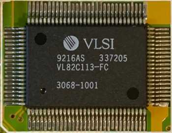
The VL82C380 is a highly integration solution. A complete system can be implemented using only the CPU, BIOS, DRAM, VL82C380, VL82C113A Combination I/O and 3 SSI TTL's, plus optional TAG and Data SRAMs.
Tag SRAMs can be either 8- or 9-bit (7- or 8-bit tag plus a dirty bit). Dirty and Valid bits are optional, each may be disabled in order to increase cacheable DRAM range. The Dirty bit, when used, indicates that the cache has been updated but not the corresponding locations in DRAM. The Valid bit, when used, indicates that both the cache and corresponding DRAM locations have been updated.
Only on-board DRAM is cached, this prevents coherency issues associated with caching system memory in the ISA bus. Full coherency is maintained during DMA/Master mode cycles, so flushing and invalidating operations are unnecessary. set-up/sizing mode (programmable) provides direct access to the cache data SRAMs.
The Memory Controller logic is capable of accessing up to 64 MB. There can be up to 4 banks of 256K, 1M, or 4M DRAMs used in the system. The VL82C380 can drive two banks without external buffering. Built-in page-mode operations and up to 2-way interleaving allow the PC designer to maximize system performance using low-cost DRAMs. Programmable DRAM timing is provided for RAS precharge, RAS to CAS delay, and CAS pulse width.
Features:
- Highly integrated system solution using VL82C380 single-chip ISA controller, VL82C113A Combination I/O chip and 3 TTLs
- Supports one- or two-bank write-back cache
- External TAGs
- 32 Kbyte to 1 Mbyte cache size
- 0 or 1 wait state writes
- Separate dirty RAM not required; first write to clean, valid line sets dirty bit
- Caches main system DRAM only
- Maintains full coherency during DMA/MASTER mode cycles
- Optional remap of video and hard disk ROM BIOS onto motherboard, allowing use of single BIOS ROM
- Optional bus acceleration for video accesses, with programmable address regions
- Software-configurable
- Utilizes proven 8254, 8237, 8259 megacalls used in all previous VLSI Technology PC/AT chipsets
- High-performance memory controller:
- One wait state red up to 33 MHz, Zero wait state reads up to 40 MHz
- Automatic configuring of Bank start address
- Each bank individually configurable for any supported DRAM type
- shadow RAM support form 640K to 1M in 16K segments
- Staggered refresh reduces power supply peak currents
- Decoupled-mode refresh improves performance
- Programmable refresh frequency for support of slow-refresh DRAMs
- Up to 64 Mbytes of motherboard memory in one to four banks using 256K, 1M, and/or 4Mbit DRAM, all motherboard memory is cacheable
- Direct-drive up to 2 banks (32 Mbyte) of motherboard memory
- Two-way page mode interleave
- Supports 32-bit ini-interleaved or interleaved configurations
- Programmable RAS/CAS timing supported for Cycle-start, Trp, Trcd, and Tacs
Disclaimer
The info found in this page might not be entirely correct. Check out this guide to learn how you can improve it.
 Image 1 of 1 (RetroShare)