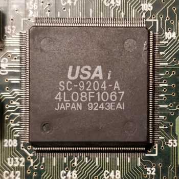
USA Integration SC-9204-A
1992-01-01
Features:
- Direct mapped organization with write-back protocol
- 0 wait state for cache read / write hit
- Programmable cache read / write hit wait state. Cache controller can be enabled or disabled
- Programmable cache line size
- Flexible cache size
- One or two bank of cache SRAM
- Flexible direct SRAM access mode
- Support for both hidden and conventional DRAM refresh
- Support for two independent non-cacheable regions
- Video and System BIOS Shadow RAM can be cacheable in either the secondary cache or the 486 internal cache
- Support of fast Gate A20 operation for optimization of OS / 2 operations
- Support for Fast / Standard page mode DRAM
- Support for 2 banks of DRAM with memory size up to 64MB
- Flexible system memory configurations
- Support mixable 256KB x 9, 1MB x 9, 4MB x 9, and 16MB x 9 SIMM modules between banks
- Programmable DRAM wait state
- Programmable cache flush
- Relocation of unused first 1 MB segments (128 KB, 256KB, or 384 KB) to top of DRAM memory
- Automatic memory size detection
- CPU interface logic
- Data bus buffer control logic
- Reset and shutdown logic
- NM1 and port B support
- Feedback CPU clock to reduce clock skew
- Support for turbo / non-turbo mode
- Support for software turbo switch
- Support for conventional / hidden refresh
- Programmable bus clock
- DMA interface and arbitration logic
- Refresh address and control logic
- Data bus conversion logic
- Bus interface between different data buses
- Parity generation and checking logic
- 14.3 18Mhz and divide 12 counter
- AT Bus I/O recovery option for slower I/O card
Chip
Release date
File
Logs
Last updated 2019-04-30T00:00:00Z
Disclaimer
The info found in this page might not be entirely correct. Check out this guide to learn how you can improve it.
 Image 1 of 1 (deksor)