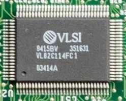
VL82C114 Combination I/O
The VL82C114 Combination I/O chip, when used with VLSI System Controller chips, allows designers to implement a very cost-effective minimum chip count motherboard. This chip combines a keyboard controller and a real-time clock with the address registers/ latches and buffers which are normally required in ISA bus compatible systems. The VL82C114 features an AT-compatible keyboard controller with integrated PS/2 mouse support and a 146818A-compatible real-time clock. The VL82C114 also has 114 additional bytes of battery-backed CMOS RAM for use in extended system setup. In addition, the VL82C114 provides support for processors with write-back cache controllers.
Features:
- Integrated peripheral controller that interfaces with several of VLSI's Single Chip System/ISA Bus controllers
- VL82C480
- VL82C481
- VL82C486
- VL82C310
- VL82C311
- VL82C311L
- Backwards compatible with the industry standard VL82C113A
- 146818A-Compatible real-time clock
- 114 additional bytes of battery-backed CMOS RAM
- AT-compatible keyboard controller with integrated PS/2 mouse support
- Processor to ISA bus address latches and buffers, which support 16- and 32-bit processors.
- Supports processors with write-back cache controllers
- Real-time clock can be relocated via SA[15:0] address registers
- Includes ISA bus refresh counters for decoupled refresh
- 1.0-micron CMOS
- 100-lead MQFP (Metric Quad Flat Pack)
Disclaimer
The info found in this page might not be entirely correct. Check out this guide to learn how you can improve it.
 Image 1 of 2 (VanoRu)
 Image 2 of 2 (Motherboard Continuum)